The Rise of Optical Communication Chips: How CRYSPACK Became the Unrivaled Choice for Chip Packaging
2026.06.02 / By cryspak
The global optical communication chip industry is experiencing an unprecedented surge. Fueled by AI workloads, 5G infrastructure, data center expansions, and emerging technologies like autonomous vehicles and quantum computing, the demand for high-speed photonic chips has skyrocketed. A market report from Yole Group projects the photonics packaging market to triple by 2031, driven by the transition from traditional optical transceivers to complex architectures like Co-Packaged Optics (CPO) and heterogeneous integration. As these sensitive, high-value components flood the supply chain, the need for reliable, high-performance protective packaging has never been more critical.
Enter CRYSPACK — a global provider of precision packaging solutions headquartered in Fuzhou, China, with over two decades of industry expertise. From elastic membrane boxes and self-adsorption boxes to advanced vacuum release trays and wafer containers, CRYSPACK offers an extensive portfolio tailored to the stringent demands of the semiconductor, photonics, and optoelectronics industries. Serving over 1,500 clients worldwide, including industry giants like Coherent, Limo, and IPG, the company has built a reputation for reliability and innovation.
A Market Primed for Specialized Protection
Optical communication chips — including silicon photonics transceivers, EMLs, VCSELs, laser diodes, and photodetectors — are among the most delicate components in electronics. They are highly susceptible to electrostatic discharge (ESD), micro-contamination, mechanical vibration, and moisture. Traditional packing methods, such as standard waffle packs and foam trays, often fail to provide adequate protection, leading to yield loss, rework costs, and compromised product integrity.
CRYSPACK‘s Technology Edge
CRYSPACK has addressed these market challenges through a suite of patented technologies and innovative product lines.
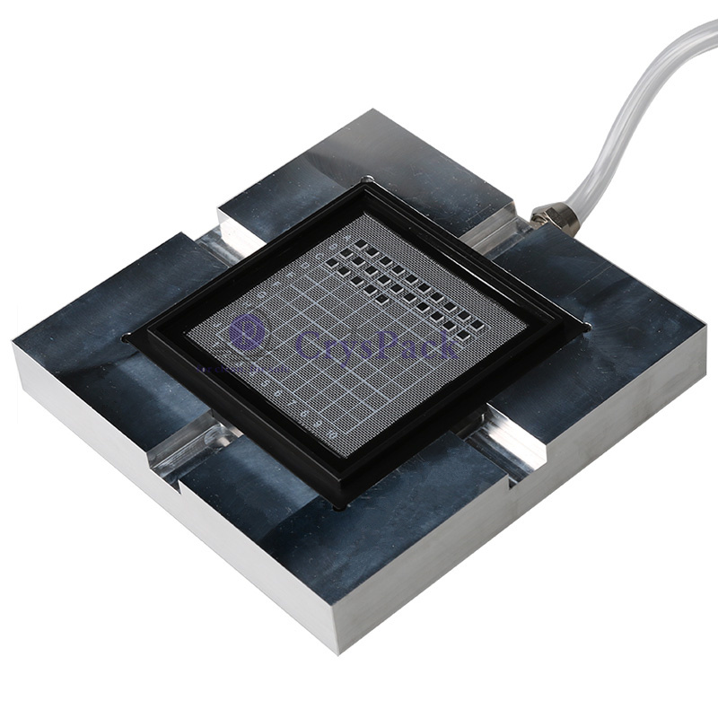
One of its flagship offerings is the Vacuum Release Tray. This technology uses vacuum sealing to secure ultra-thin and fragile chips without direct physical contact, effectively preventing damage during transit. The tray is constructed from electrically conductive material in a sleek black finish, providing superior ESD protection and thermal management — ideal for high-speed photonic devices sensitive to static charges.
Another breakthrough is the Recyclable ESD Gel Sticky Carrier, which features a conductive tray embedded with a static dissipative polyurethane film. This carrier not only neutralizes static charge but also comes with various tack levels, enabling customized immobilization for chips as small as bare die.
For optical components and lenses, CRYSPACK offers Static Dissipative Membrane Boxes and Optical Storage Boxes. The membrane boxes utilize highly elastic transparent films that suspend irregularly shaped components in mid-air, protecting them while allowing visual inspection without opening the package. Meanwhile, the optical storage boxes are built from low-outgassing PET-G material, ensuring cleanroom compatibility and safeguarding optics from scratches, dust, and harmful pollutants.
Meeting the Demands of Co-Packaged Optics and AI
As the industry moves toward CPO and 3D integration, where photonics chips are integrated directly with electronics, packaging requirements are evolving beyond mere containment. CRYSPACK‘s wafer containers and custom VR plates are specifically designed to handle fragile substrates like InP, GaAs, and GaN wafers — essential materials for next-generation optical engines. The company is also aligning with sustainability trends by introducing recyclable materials without compromising high-barrier protection.
A Trusted Partner for the Global Photonics Supply Chain
CRYSPACK’s success lies in its ability to provide fully customizable, cleanroom-compatible packaging at competitive lead times. With ISO9001-certified manufacturing processes, in-house mold design and over 30 patents, the company ensures that every chip container meets the rigorous demands of automated pick-and-place equipment and high-mix, low-volume production lines.
As photonics packaging matures from a niche logistics afterthought to a strategic enabler of chip reliability, CRYSPACK has positioned itself at the forefront of this transformation. The company‘s active participation at global events like SPIE Photonics West 2026 underscores its commitment to driving innovation and serving the semiconductor ecosystem.
Conclusion
The explosive rise of the optical communication chip industry is not just a triumph for data speed — it’s a catalyst for change across the entire packaging value chain. For manufacturers seeking to protect their billions of dollars of photonics investments, the choice is clear. With two decades of expertise, a comprehensive product range, and a proven track record with global leaders, CRYSPACK has become the premier and trusted solution for chip storage and transportation in the age of optical computing.