Laser Chip Packaging
2024.05.30 / By admin
Meta Descriptions
Explore CrysPack’s laser chip packaging options for safe and efficient storage solutions. Trust our expertise for your packaging needs.
What Are the Key Considerations in Laser Chip Packaging Design?
In the fast-paced world of semiconductor manufacturing, the chiplet trend has emerged as a revolutionary approach. This trend involves breaking down large, monolithic functionalities into interconnected smaller dies, offering advantages such as improved flexibility, scalability, and reduced time to market compared to the traditional System on Chip (SoC) approach.
The Rise of Chiplets
1. Breaking Down Monolithic Functionalities: Chiplets represent a departure from the conventional monolithic approach by breaking down complex functionalities into smaller, interconnected dies. This modular design enables greater flexibility in customization and optimization for specific applications.
2. Advantages over SoC: Unlike System on Chip (SoC) designs, which integrate all components onto a single die, chiplets allow for independent development and testing of each component. This not only enhances scalability but also simplifies the design process and reduces manufacturing costs.
The Importance of Known Good Die (KGD)
1. Ensuring Quality and Reliability: With the adoption of chiplets, there’s a heightened demand for Known Good Die (KGD). These are dies that have undergone comprehensive testing to ensure they meet quality standards before integration into their final packaging. Ensuring the quality of each die is crucial for maintaining overall chip performance and reliability.
2. Quality Control Challenges: Achieving KGD status for chiplets poses significant challenges due to the diverse range of device dimensions and the need for meticulous testing processes. Laser technology plays a crucial role in addressing these challenges by enabling precise testing and inspection of individual dies.
Challenges in Test and Assembly
1. Handling Diverse Device Dimensions: Conventional methods for handling chips face challenges in the test and assembly processes of chiplets due to the multitude of device dimensions. Laser technology offers a solution by providing precise and versatile tools for handling various chip sizes and configurations.
2. Pick-and-Place Efficiency: The traditional pick-and-place assembly process can be inefficient when dealing with chiplets, as it may require multiple pick-and-repick cycles or transfer between processes. Laser chip packaging streamlines this process by offering high-speed and accurate placement of chiplets onto substrates.
3. Thermal Management: Efficient thermal management is essential for maintaining the reliability and performance of chiplets. Laser technology enables the integration of advanced thermal solutions directly into the chip packaging, ensuring optimal heat dissipation and reliability under demanding operating conditions.
Addressing Complexity in Test and Assembly
1. Challenges in Conventional Methods: Traditional methods of chip handling struggle to cope with the intricacies of chiplet integration. The multitude of components and the need for precise alignment present significant hurdles in test and assembly processes.
2. Streamlining with Laser Technology: Laser chip packaging revolutionizes test and assembly processes by leveraging precision laser technology. This approach simplifies chiplet handling, reducing the risk of errors and improving overall efficiency.
Precision and Efficiency in Handling
1. Accurate Placement and Bonding: Laser chip packaging provides unparalleled precision in the placement and bonding of chiplets. Laser beams can be precisely controlled to ensure the accurate positioning of components, minimizing the risk of damage or misalignment during assembly.
2. Minimizing Assembly Time: The efficiency of laser technology enables rapid handling and bonding of chiplets, reducing assembly time and improving overall productivity. This precision and speed are crucial for meeting the demands of modern semiconductor manufacturing.
Enhancing Flexibility and Scalability
1. Seamless Integration of Diverse Configurations: Laser chip packaging enhances flexibility by enabling the seamless integration of diverse chiplet configurations. Whether it’s different sizes, shapes, or functionalities, laser technology can accommodate various chiplet specifications with ease.
2. Facilitating Rapid Prototyping: The flexibility offered by laser chip packaging allows semiconductor manufacturers to expedite the prototyping process. By quickly adapting to different chiplet configurations, manufacturers can iterate designs more efficiently and bring products to market faster.
3. Scalability for Mass Production: Laser technology is not only suitable for prototyping but also for mass production. Its scalability enables high-volume manufacturing without compromising precision or efficiency, making it an ideal solution for semiconductor companies of all sizes.
Introducing CrysPack: Innovating Laser Chip Packaging
1. Pioneering Laser Technology: CrysPack is at the forefront of innovation in laser chip packaging, leveraging cutting-edge laser technology to address the unique challenges of chiplet integration. By combining precision, speed, and versatility, CrysPack’s solutions enable efficient testing, assembly, and packaging of chiplets with uncompromising quality and reliability.
2. Customized Solutions: Recognizing the diverse needs of semiconductor manufacturers, CrysPack offers customized laser packaging solutions tailored to specific chiplet applications. Whether it’s high-volume production or prototyping, CrysPack’s team of experts works closely with clients to develop bespoke solutions that meet their exact requirements.
3. Advancing Semiconductor Manufacturing: Through continuous research and development, CrysPack is driving advancements in semiconductor manufacturing, pushing the boundaries of what’s possible with laser technology. By providing state-of-the-art solutions for chiplet packaging, CrysPack is empowering semiconductor companies to stay ahead in a competitive market landscape.
Protecting Fragile Innovations: The Superiority of CrysPack Laser Chip Packaging
1. Innovative Packaging Solutions
At the heart of CrysPack’s offerings lies a diverse portfolio of packaging solutions designed to cater to the specific needs of various industries. The company’s commitment to research and development has yielded several series of products, each meticulously crafted to address unique challenges.
2. Membrane Boxes: Unmatched Flexibility
Among CrysPack’s offerings, Membrane Boxes stand out as a testament to innovation and versatility. Constructed with a thin, highly elastic transparent film, these boxes provide the perfect solution for devices or objects with irregular shapes or non-flat contact surfaces. By ensuring a snug fit and secure enclosure, Membrane Boxes offer unparalleled protection during transit and storage.
3. Sticky Box: Securing Fragile Components
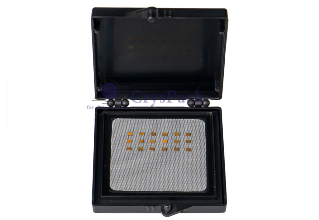
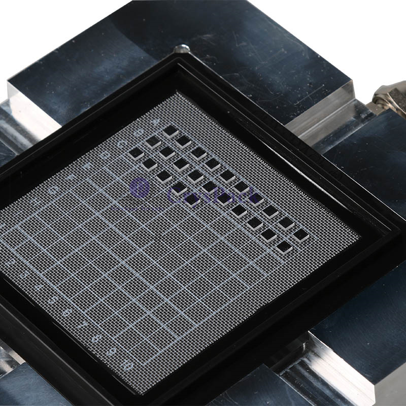
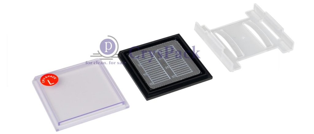
For tiny and delicate devices requiring extra stability during transportation, CrysPack’s Sticky Box comes to the rescue. Comprising a plastic hinged box coated with a special gel on the bottom, this solution effectively fixes delicate components in place, minimizing the risk of damage or displacement.
4. Vacuum Box: Preserving Fragility
In the realm of laser chip packaging, fragility is a constant concern. CrysPack’s Vacuum Box presents an innovative solution to this challenge. By creating a controlled vacuum environment within the packaging, this solution ensures the safe transit and storage of extremely fragile or thin devices, safeguarding them from external stressors.
5. Optic Storage Boxes: Ensuring Pristine Optics
Cleanliness and protection are paramount when it comes to optics. CrysPack’s Optic Storage Boxes are purpose-built to keep optics clean and damage-free during storage or transport. With airtight seals and robust construction, these boxes provide the ideal environment for preserving the integrity of sensitive optical components.
6. Wafer Container: Safeguarding Semiconductor Wafers
Semiconductor wafers are the backbone of modern electronics, and their packaging demands meticulous attention to detail. CrysPack’s Wafer Container offers a reliable packaging solution tailored specifically for semiconductor wafers, ensuring their safe transit and storage from production facility to end-user.
7. Custom Solutions: Tailored to Perfection
Beyond its standard product offerings, CrysPack prides itself on its ability to design and manufacture custom packaging solutions to meet the unique requirements of its clients. With a focus on quality, efficiency, and customer satisfaction, the company collaborates closely with its clients to deliver bespoke packaging solutions that exceed expectations.
Conclusion
As the semiconductor industry continues to evolve, the adoption of chiplet technology represents a paradigm shift in design and manufacturing methodologies. With its unparalleled precision, speed, and versatility, laser chip packaging is poised to play a pivotal role in enabling the seamless integration of chiplets into next-generation electronic devices. As a leading provider of laser packaging solutions, CrysPack is committed to driving innovation and pushing the boundaries of semiconductor manufacturing, ushering in a new era of performance and reliability.