
 Chinese
Semiconductor devices are the backbone of modern technology, powering everything from smartphones to industrial machinery. However, these devices are incredibly delicate and susceptible to damage from electrostatic discharge (ESD) during shipping, handling, and processing. To address this challenge, CrysPack introduces its revolutionary Recyclable ESD Gel Sticky Carrier, a cutting-edge solution designed to securely hold fragile devices, including bare die, while providing effective ESD protection throughout the manufacturing process.
Understanding ESD and Its Impact on Semiconductor Devices
1.1 The Science Behind Electrostatic Discharge
Static electricity, or electrostatic charge, is a common phenomenon wherein stationary charges accumulate on the surface of materials. The interaction between these charges can lead to two significant problems in semiconductor devices: electrostatic overstress (EOS) and electrostatic discharge (ESD). ESD, in particular, accounts for more than one-third of field failures in the semiconductor industry. It manifests as various types of damage, including leakage, short circuits, burnout, and gate oxide rupture.
The Importance of ESD Protection in Semiconductor Manufacturing
2.1 Challenges Posed by ESD Sensitivity
The shrinking size of semiconductor chips and the complexity of modern integrated circuits exacerbate their susceptibility to ESD damage. With CMOS scaling reducing power and increasing speed, the thinner gate oxides are more prone to damage under EOS/ESD conditions. Predicting and mitigating ESD events is challenging due to their occurrence at both microscopic and macroscopic levels.
2.2 Effective ESD Protection Strategies
To minimize the risk of ESD-induced failures, two primary strategies are employed in semiconductor manufacturing. First, ensuring proper handling and grounding of personnel and equipment during all stages of production, transportation, and application of ICs is crucial. Second, incorporating on-chip protection circuits to divert high currents away from internal circuitry and clamp high voltages during an ESD event can significantly enhance device robustness.
2.3 The Role of Failure Analysis in ESD Mitigation
Analyzing field return devices provides valuable insights into failure mechanisms, guiding the design and development of more resilient semiconductor products. While chip manufacturers adhere to industry standards for ESD qualification, they cannot control how customers handle their devices. Hence, effective on-chip circuit protection and rigorous testing are essential to ensure device reliability in real-world environments.
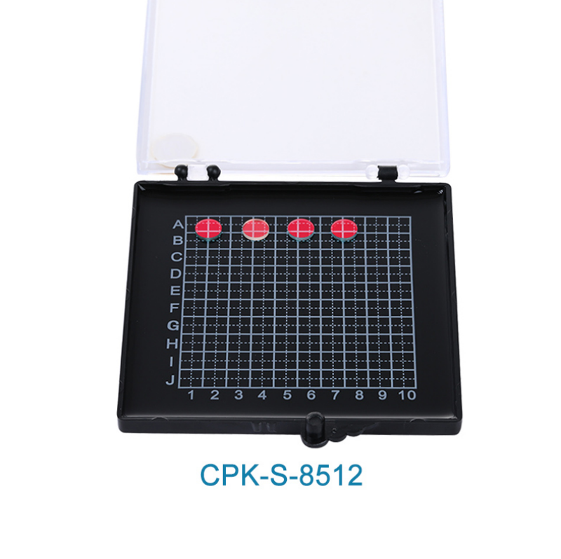
Features and Applications of the Recyclable ESD Gel Sticky Carrier
3.1 Conductive Tray with Static Dissipative Polyurethane Film
The Recyclable ESD Gel Sticky Carrier from CrysPack features a conductive tray embedded with a static dissipative polyurethane film. This innovative combination provides comprehensive ESD protection by effectively dissipating static charges and preventing their accumulation on the carrier’s surface.
3.2 Versatile Sizing Options and ESD Film Tack Levels
CrysPack offers the Recyclable ESD Gel Sticky Carrier in a variety of sizes to accommodate different semiconductor devices, including bare die. Additionally, customers can choose from various ESD film tack levels, allowing for customized solutions tailored to specific application requirements.
3.3 Sustainable and Environmentally Friendly Design
As the name suggests, the Recyclable ESD Gel Sticky Carrier is designed with sustainability in mind. Its recyclable materials ensure minimal environmental impact, aligning with the growing demand for eco-friendly packaging solutions in the semiconductor industry.
3.4 Automated Pick & Place Compatibility
Ideal for automated pick & place applications, the Recyclable ESD Gel Sticky Carrier facilitates seamless handling and processing of fragile semiconductor devices. Its vacuum release tray allows for easy offloading of devices by applying vacuum to the underside of the carrier, streamlining manufacturing workflows and improving operational efficiency.
Understanding Charge Generation and Transfer Mechanisms
4.1 Triboelectric Charging: The Origin of Static Electricity
Triboelectric charging, induced by friction between different materials, is a primary mechanism behind static electricity generation. When two materials come into contact and separate, one material may lose electrons (positively charged) while the other gains electrons (negatively charged), resulting in a charge imbalance. This phenomenon, known as triboelectricity, is prevalent in various scenarios, including personnel walking across floors or semiconductor components sliding during transportation.
4.2 Induction and Conduction: Additional Paths to Charge Generation
In addition to triboelectric charging, electrostatic charge can be induced in materials when brought near charged objects, leading to a distributed charge distribution. Conduction occurs when charged bodies of differing potentials come into contact, causing charge transfer until equilibrium is reached. Understanding these mechanisms is crucial for developing effective ESD mitigation strategies in semiconductor handling environments.
4.3 Material Classification for ESD Handling
Materials can be classified based on their ability to dissipate static charge effectively. Categories include insulators, slow charge dissipative anti-static materials, charge dissipative anti-static materials, and conductive materials. Anti-static and dissipative materials are commonly used in semiconductor manufacturing to limit charge buildup and mitigate ESD risks.
The Impact of EOS on Semiconductor Reliability
5.1 Thermal Damage and Device Degradation
EOS, characterized by current or voltage beyond device specification limits, poses a significant threat to semiconductor reliability. High currents during EOS events generate excessive heat, leading to localized temperature spikes and material damage. Gate oxide rupture, interconnect burnout and junction breakdown are among the common failure modes associated with EOS.
5.2 Differentiating ESD and EOS
While ESD and EOS share similarities in stress events, their characteristics differ in terms of voltage, current, and duration. ESD events involve high-voltage, moderate-current discharges over a short timeframe, whereas EOS events entail lower-voltage, high-current discharges over a longer duration. Understanding these distinctions is essential for implementing effective protection measures.
5.3 Latchup and Extended Stress Conditions
Latchup, a phenomenon where a parasitic structure in an integrated circuit causes unintended conduction paths, can exacerbate EOS damage if sustained over time. Extended stress conditions, whether from ESD or EOS, may result in latent defects that manifest as functional failures after prolonged operation, posing challenges for reliability testing and detection.
CrysPack’s Recyclable ESD Gel Sticky Carrier: Features and Benefits
6.1 Secure Handling and ESD Protection
CrysPack’s Recyclable ESD Gel Sticky Carrier provides a secure platform for handling fragile semiconductor devices, including bare die, during shipping, handling, and processing. The vacuum release tray allows for easy offloading of devices by applying vacuum to the underside of the carrier, minimizing the risk of damage from manual handling.
6.2 Conductive Tray with Static Dissipative Film
The carrier is constructed with a conductive tray and static dissipative polyurethane film, ensuring effective ESD protection with a surface resistance of < 10^9 ohms. This combination dissipates static charges and prevents their accumulation, safeguarding semiconductor components from ESD-induced failures.
6.3 Versatile Sizing and Tack Level Options
CrysPack offers the Recyclable ESD Gel Sticky Carrier in a variety of sizes and ESD film tack levels, catering to diverse application requirements. Whether for automated pick & place operations or manual handling, customers can choose the appropriate carrier configuration to suit their specific needs.
Conclusion
In conclusion, CrysPack’s Recyclable ESD Gel Sticky Carrier represents a significant advancement in semiconductor packaging technology, offering robust ESD protection, versatility, and sustainability in one innovative solution. By addressing the challenges posed by ESD sensitivity, this cutting-edge carrier ensures the safe and reliable handling of fragile semiconductor devices throughout the manufacturing process.
Post time: Mar-15-2024